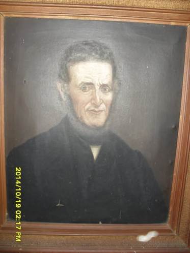
Following the Evans thread this morning I came upon my great grandmother Annie Morgan. Who was born in Schulkil County Pennsylvania in 1890.
In the 1891 census they are back in Aberdare. Her parents must have popped over there between 1881 and 1891…It turns out she was the first teacher in the family…
Perhaps they offered some Welsh coal mining expertise… the family is all about steel and coal.
Around forty years ago we had a visit whilst in Wales from two American women claiming to be relatives.
Perhaps when David and Elizabeth were in Pennsylvania they were staying with relatives in or near the so called Welsh Tract…
Does this mean that I can claim American citizenship by birth?
Far out…
——————————————————————-
These below excerpted from Wikipedia
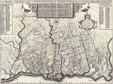
The Welsh Tract, also called the Welsh Barony, was a portion of the Province of Pennsylvania, a British colony in North America (today a U.S. state), settled largely by Welsh-speaking Quakers in the late 17th century. The region is located to the west of Philadelphia. The original settlers, led by John Roberts, negotiated with William Penn in 1684 to constitute the Tract as a separate county whose local government would use the Welsh language. The Barony was never formally created, but the many Welsh settlers gave their communities Welsh names that survive today. A more successful attempt at setting up a Gwladfa (Welsh-speaking colony) occurred two centuries later, in the Chubut Province of Patagonia, Argentina.
–
–
Thomas Holme’s 1687 map of Pennsylvania. “The Welch Tract” appears to the left of center.
Prior to the arrival of Welsh settlers, the land of what would become the Welsh Tract was inhabited by Indigenous peoples, such as the Okehocking band of the Lenape.
————-
Schuylkill County is a county in the Commonwealth of Pennsylvania. As of the 2020 census, the population was 143,049. The county seat is Pottsville. The county is part of the Northeast Pennsylvania region of the state.
The county is part of the Pottsville micropolitan statistical area, and borders eight counties: Berks and Lebanon counties to its south, Dauphin and Northumberland counties to its west, Columbia and Luzerne counties to its north, and Carbon and Lehigh counties to its east. The county is approximately 47 miles (76 km) west of Allentown, the state’s third-largest city, and 97 miles (156 km) northwest of Philadelphia, the state’s largest city.
The county was created on March 1, 1811, from parts of Berks and Northampton counties and named for the Schuylkill River, which originates in the county. On March 3, 1818, additional territory in its northeast was added from Columbia and Luzerne counties.
—-
19th century
Schuylkill County was created via an Act of Assembly on March 1, 1811, from portions of Berks and Northampton counties. More land was added to the county in 1818, from Columbia and Luzerne counties. At the time of its creation, the county had a population of about 6,000.
————
The numerous jobs in the mining industry comprised a catalyst for mass immigration to Schuylkill County from the British Isles and Europe in the 19th and 20th centuries. As mines became more numerous (by 1846 there were 110 operators in the region and 142 collieries in Schuylkill County) and more complex (in 1846 there were 35 collieries below water level), mechanical breakers, steam locomotive, it became more labour-intensive both for accomplishing mining tasks and supporting mining’s peripheral industries. Such industries included manufacturing of explosives, metal screens, pump components, piping, and timber for support. This led to an influx of population into Schuylkill and other anthracite counties to fill these jobs.
Beginning with the Irish immigration in the 1840s, which was fuelled by the Great Famine and followed the end of the Civil War, immigrants from Eastern Europe, including Poles, Hungarians, Lithuanians, Slovaks, Rusyns, Ukrainians, and Belarusians (which were usually known as Ruthenians), often from the Austro-Hungarian monarchy, settled in Schuylkill County and laboured in the county coal mines. By the 1880s and 1890s, thousands of Italians immigrated to the county in pursuit of mining jobs.